Impedance Equalization on PCB Traces
A Critical Step for High-Frequency Designs
In today's electronic designs, especially in circuits requiring high-frequency and fast data transmission, impedance equalization has become a crucial design requirement. Impedance equalization maintains signal integrity while minimizing issues like reflections, loss, and electromagnetic interference (EMI). So, what exactly is impedance equalization, and how is it implemented in PCB designs?
What is Impedance and Why is it Important?
Impedance is the resistance a conductor offers to AC signals, and in PCB designs, it depends on factors such as the physical dimensions of the traces, the materials used, and the frequency of the signal. For high-frequency signals, if the trace impedance is not compatible with the impedance of the source and load, the following problems arise:
- Signal Reflection: Impedance mismatch can cause signal reflection and distortion.
- Signal Delay: Impedance differences cause the signal to reach the destination late.
- Data Loss: Increases the error rate, especially in high-speed data protocols.
- EMI and Interference: May increase the effect of environmental electromagnetic interference sources.
What is Impedance Equalization?
Impedance equalization is a design process that aims to maintain a constant characteristic impedance (Z0Z_0Z0) across the entire length of a PCB trace. Especially in high-speed signal paths, matching the impedance from source to load maintains signal integrity and increases system reliability.
Characteristic Impedance Calculation
The characteristic impedance of a path is calculated by the formula:
Here:
- : Characteristic impedance (Ω),
- : Dielectric constant of PCB,
- : Dielectric layer thickness,
- : Road width,
- : Copper thickness.
Application Areas of Impedance Equalization
Impedance equalization is critical in the following situations:
- High Speed Data Transmission: Protocols such as Ethernet, HDMI, USB, PCIe.
- Differential Signals: High speed dual line signals such as LVDS, DDR.
- RF Circuits: High frequency antennas and radio frequency designs.
- Clock Signals: In systems requiring precise timing.
How to Perform Impedance Equalization in PCB Design?
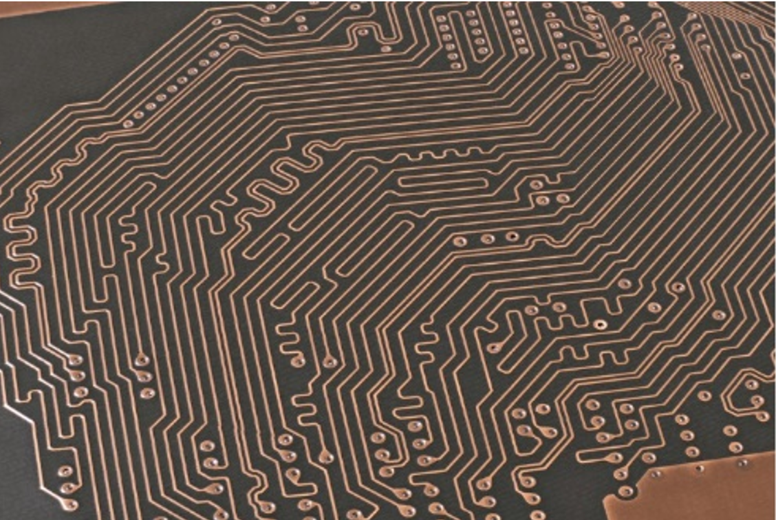
1. Road Width Adjustment
PCB trace width () is the most important determinant of impedance. Narrow traces increase impedance, while wide traces decrease impedance. You can determine the correct width using impedance calculation tools in design software (e.g., Altium or Proteus).
2. Land Plan and Distance
As the distance () between the ground plane under the road and the road decreases, the impedance decreases. For better signal quality, work as close to the ground plane as possible.
3. Differential Double Lines
For differential signals, the impedance between the two signal lines must be equalized. This impedance is typically targeted at 100Ω or 90Ω. Carefully adjust the distance (coupling) between the lines.
4. Material Selection
Common PCB materials such as FR4 have a dielectric constant ( ) of approximately 4.5. At higher frequencies, materials with lower dielectric loss should be selected.
Advantages of Impedance Equalization
- Increased Signal Quality: Signal distortions are minimized.
- Less EMI: Electromagnetic interference is reduced.
- Data Security: The error rate is reduced, especially in digital data lines.
- Higher Frequency Capability: Provides more reliable operation in high-speed designs.
Conclusion
Impedance equalization is a fundamental requirement for ensuring signal integrity in modern PCB designs. Especially in high-frequency and high-speed circuits, accurate impedance equalization is critical to your device's reliability and performance. Accurate calculations and appropriate materials selection during design simplify this process.
